What Is a Semiconductor Process Node?
A process node like '5nm' or '3nm' names a chipmaker's manufacturing generation, not a literal measurement anymore. Here's what the number means.
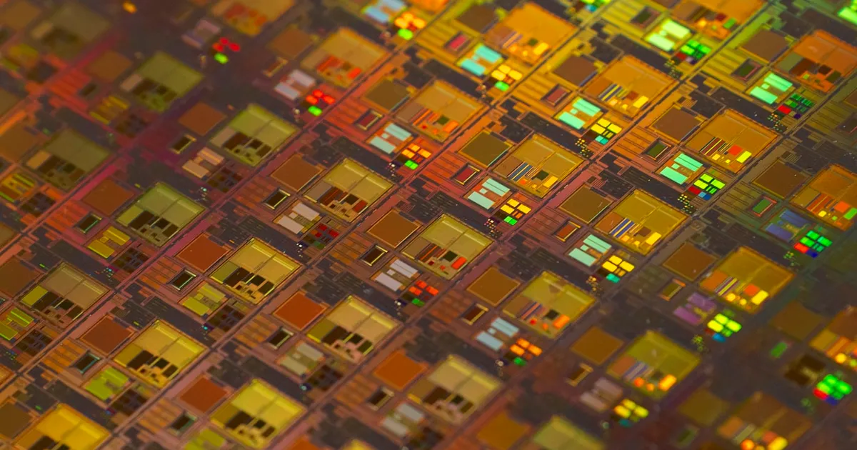
A process node (or “process technology”) names a generation of semiconductor manufacturing — you’ve seen it as “5nm,” “3nm,” or “2nm” attached to a chip announcement. The number originally referred to a specific physical measurement on the chip, but for well over a decade it’s functioned mainly as a marketing and generational label rather than a literal dimension you could measure with a ruler.
What the nanometer number used to mean
In older manufacturing generations, the node number referred to the transistor’s gate length — a specific, measurable feature size on the chip. A “90nm” chip really did have transistor gates around 90 nanometers long, and smaller numbers reliably meant smaller, denser, more efficient transistors.
That direct correspondence broke down as transistor geometry got more complex. Modern transistors (FinFET and newer gate-all-around designs) aren’t simple planar structures with one obvious length to measure, so there’s no single physical dimension the node name could accurately describe anymore. Different manufacturers now define their node names using their own internal conventions, which is why comparing “5nm” from one foundry to “5nm” from another isn’t a straightforward apples-to-apples comparison — they’re both marketing names for a manufacturing generation, not identical measurements.
What actually improves between nodes
Even though the number itself isn’t literal, moving to a new node generation is still real and still matters — it typically brings some combination of:
- Higher transistor density — more transistors fit in the same silicon area, which is what lets a new chip generation pack more compute into the same physical footprint.
- Lower power consumption per transistor — meaningful for battery-powered devices and for data centers where power and cooling are a major cost driver.
- Higher achievable clock speeds — not guaranteed, but a smaller, more efficient transistor generally has more thermal headroom to run faster.
None of these move in lockstep, and a new node doesn’t automatically deliver all three — a foundry’s own published node roadmap typically emphasizes whichever tradeoff (density, power, or speed) a given generation is optimized for.
Why smaller nodes are so much harder to build
Each new node generation requires more advanced manufacturing equipment, and the transition to EUV lithography was largely driven by the fact that older lithography techniques physically couldn’t pattern features small enough for nodes below roughly 7nm-class generations. That’s a large part of why only a small handful of companies in the world (chiefly TSMC, Samsung, and Intel) can manufacture at the leading edge — the capital cost of a fab capable of the smallest current nodes is enormous, and it keeps climbing with each generation.
This is also why fabless chip designers — companies that design chips but don’t manufacture them — depend so heavily on a small number of foundry partners, and why a foundry’s node roadmap and yield rates are closely watched signals in the industry: a delayed or low-yield node can bottleneck an entire generation of products across many companies at once.
Node names vs actual performance
| What it reliably tells you | What it doesn’t | |
|---|---|---|
| Node name (e.g. “3nm”) | Roughly which generation of manufacturing was used | A literal transistor dimension |
| Cross-foundry comparison | Not directly comparable | Two foundries’ “3nm” can differ meaningfully in real density |
| Real-world chip performance | Correlated, but not determined by the node alone | Depends heavily on chip architecture, not just the manufacturing process |
This is why two chips built on the “same” node from different designers can perform very differently — architecture, memory subsystem, and how efficiently the design uses the available transistor budget all matter as much as the node itself. It’s also why comparing chips purely by process node name, without looking at actual benchmarks or specifications, tends to be misleading.
Where this fits with related hardware concepts
Process node improvements are the physical engine behind the broader trend historically described by Moore’s Law — the observation that transistor density on a chip roughly doubles on a predictable cadence. As node scaling has gotten physically harder and more expensive, that cadence has slowed, which is part of why chip designers increasingly lean on architectural tricks — chiplets, specialized accelerators like NPUs and TPUs — to keep delivering performance gains that a shrinking node alone can no longer guarantee.
The takeaway
A process node’s name — “5nm,” “3nm,” and so on — is a generational label for a manufacturing process, not a literal, directly comparable physical measurement, and hasn’t been for years. What actually matters is the real-world outcome a new node delivers: higher transistor density, lower power draw, or higher achievable clock speeds, none of which move together automatically. When comparing chips, treat the node name as a rough generational marker and look at actual specifications and architecture for anything more precise.
Tagged
Keep reading
 Chisato · · 5 min read
 What Is a Memory Controller?
A memory controller is the circuit that manages every read and write between the CPU and main memory, setting the ceiling on bandwidth and latency.
 Chisato · · 4 min read
 What Is a DPU (Data Processing Unit)?
A DPU is a specialized chip that offloads networking, storage, and security tasks from the CPU. How data processing units fit alongside CPUs and GPUs.
 Chisato · · 5 min read
 RISC vs CISC: Instruction Set Architectures Explained
RISC and CISC are two philosophies for CPU instruction sets — simple fixed-length instructions versus fewer, complex ones. How they differ and why.