What Is EUV Lithography? Chipmaking's Key Process Explained
EUV lithography uses 13.5nm-wavelength light to etch the finest features on modern chips. How it works and why it's a chokepoint in chip manufacturing.
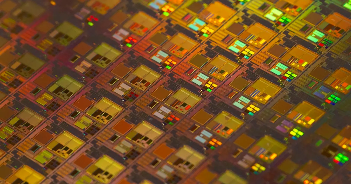
EUV lithography — extreme ultraviolet lithography — is the manufacturing process that uses very short-wavelength light to etch the finest, most densely packed features onto a silicon wafer. It’s the technology that made it possible to keep shrinking transistors after older lithography techniques ran into physical limits, and it’s produced by essentially a single company in the world, which makes it one of the most consequential chokepoints in the entire chip supply chain.
What lithography actually does
Chip manufacturing builds up a processor or memory chip in layers, and each layer’s pattern — the maze of transistors and wiring — gets defined through photolithography: light is projected through a stencil-like template called a photomask, and it passes through a lens system that focuses and shrinks the pattern onto a wafer coated in a light-sensitive material called photoresist. Wherever light hits, the resist’s chemical properties change, and a subsequent etching step uses that change to carve the actual pattern into the layer below. Repeat this dozens of times, with different masks for each layer, and the layers stack into a finished chip.
The smallest feature this process can reliably print is fundamentally limited by the wavelength of the light used — shorter wavelengths can focus onto smaller spots, the same way a finer pen tip lets you draw a thinner line. This is the physics that eventually forced the industry to move to EUV.
Why 13.5 nanometers
Before EUV, chipmakers used deep ultraviolet (DUV) light at a 193-nanometer wavelength — and pushed that technology remarkably far past its apparent limits using tricks like multi-patterning (splitting one dense layer’s pattern across several separate exposure and etch cycles) and immersion lithography (using water between the lens and wafer to bend light further). But those workarounds add manufacturing steps, cost, and complexity, and they eventually stopped being able to keep up with the feature sizes needed for further transistor shrinks — the kind of progress captured by Moore’s Law.
EUV light has a wavelength of roughly 13.5 nanometers — more than ten times shorter than DUV — which lets it resolve much finer features directly, without stacking as many multi-patterning steps on top. That’s the core value proposition: fewer process steps to hit a given feature size, at a density DUV alone can no longer reach economically.
Why EUV machines are so hard to build
Generating 13.5nm light and getting it to a wafer intact is dramatically harder than it sounds, for two compounding reasons.
Generating the light. EUV light at that wavelength doesn’t come from a simple lamp or laser directly — it’s produced by firing a high-powered laser at microscopic droplets of molten tin, tens of thousands of times per second, vaporizing each droplet into a plasma that emits EUV light as it cools. Producing enough usable light this way, reliably, at production speed, took the industry roughly two decades of dedicated development to make commercially viable.
Getting the light to the wafer. EUV light at 13.5nm is absorbed by essentially everything, including air and ordinary glass lenses. That means the entire optical path — from the plasma source, through mirrors that replace conventional glass lenses, to the wafer — has to operate in a vacuum, and every mirror has to be a nearly atomically perfect reflector, since even a small amount of light loss at each of several mirror bounces compounds into a large loss by the time light reaches the wafer.
The result is a machine that is less like a piece of factory equipment and more like a room-sized scientific instrument: it takes years to manufacture one unit, and only one company — ASML, based in the Netherlands — makes them at all. That single-supplier situation is why EUV access has become a genuine geopolitical chokepoint: whichever fabs can get EUV machines can produce the most advanced chips — including the GPUs that power modern AI data centers — and export controls on EUV equipment have direct, outsized effects on which countries can build leading-edge fabs.
Where EUV fits in a fab
Not every layer of a modern chip needs EUV — a chip’s layers vary enormously in how fine their features need to be, and older DUV tools remain the more cost-effective choice for the many layers that don’t require EUV’s resolution. Fabs typically mix both: EUV for the handful of critical, most densely patterned layers, and DUV for the rest. This is one reason leading-edge fab construction is so capital-intensive — a single fab needs a large fleet of both machine types, with EUV tools representing an outsized share of the total equipment cost despite handling a minority of the layers.
EUV vs DUV lithography
| DUV (193nm) | EUV (13.5nm) | |
|---|---|---|
| Wavelength | 193 nanometers | ~13.5 nanometers |
| Resolving fine features alone | Requires multi-patterning for the densest layers | Resolves them more directly |
| Optical path | Can use conventional lenses, no vacuum required | Requires mirrors and a full vacuum path |
| Light source | Excimer laser | Laser-vaporized tin plasma |
| Supplier landscape | Multiple manufacturers | Effectively one (ASML) |
| Typical use in a fab | Most layers | The handful of most critical, densest layers |
The takeaway
EUV lithography’s shorter, 13.5-nanometer wavelength lets fabs pattern the finest layers of a chip with fewer manufacturing steps than pushing older DUV technology to its limits, which is what has kept transistor density scaling moving forward. The physics required to generate and route that wavelength of light — plasma-based light sources, all-mirror vacuum optics — makes the machines themselves extraordinarily difficult to build, concentrated in a single supplier, and central to why leading-edge chip manufacturing capacity is so geographically and geopolitically concentrated.
Keep reading
 Chisato · · 4 min read
 Wafer-Scale Integration Explained
Wafer-scale integration builds one giant chip from an entire silicon wafer instead of cutting it into dies. How it works and its tradeoffs.
 Chisato · · 4 min read
 What Is HBM? High Bandwidth Memory Explained
HBM stacks DRAM dies vertically and connects them through a wide interface, trading capacity per chip for far higher bandwidth than standard DRAM.
 Chisato · · 4 min read
 What Is Dennard Scaling? Why Clock Speeds Stopped Climbing
Dennard scaling held that shrinking transistors kept power density constant, letting clock speeds rise for free. Its breakdown reshaped chip design.