What Is a Chiplet? Modular Chip Design Explained
A chiplet is a small, self-contained die that's packaged together with others to form one chip. How chiplets work and why the industry moved to them.
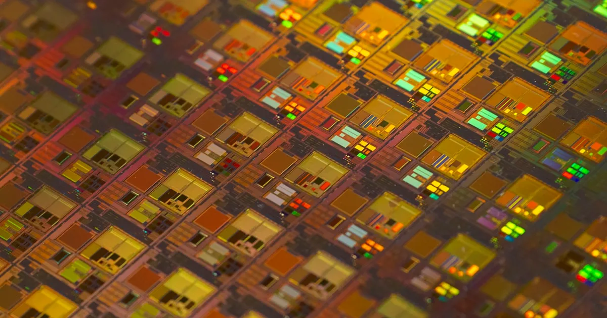
A chiplet is a small, self-contained piece of silicon that handles one part of a chip’s overall function — say, just the CPU cores, or just the I/O — and is packaged together with other chiplets to form what behaves as a single, larger chip. Instead of manufacturing one enormous piece of silicon (a “monolithic” die) that does everything, chip designers split the design into smaller dies and stitch them back together at the packaging stage. It’s the semiconductor industry’s answer to a problem monolithic dies couldn’t scale past: yield.
The yield problem chiplets solve
Chips are manufactured on large circular silicon wafers, and no fabrication process is defect-free — random flaws are scattered across every wafer. The bigger a single die is, the more likely it is to contain one of those flaws, and a single flaw ruins the whole die. This relationship is brutal at large sizes: doubling a die’s area more than doubles the odds it contains a defect, because there’s more area for a flaw to land in.
That means a giant monolithic die has a much lower yield — the percentage of dies on a wafer that come out defect-free — than several small dies covering the same total area. A defect that would kill an entire large chip only kills one small chiplet, and the rest of the wafer’s chiplets remain usable. Splitting a design into chiplets is fundamentally a way to keep yields high (and cost per working chip low) as designs grow more complex, rather than continuing to bet everything on one increasingly fragile piece of silicon.
How chiplets connect
The chiplets that make up a finished processor aren’t just sitting next to each other on a circuit board — they’re bonded together in the same package, connected by extremely short, extremely fast interconnects that behave almost like traces on a single die. This is the part that makes the split invisible to software: from the outside, a chip built from four chiplets looks and behaves like one chip.
A few packaging approaches make this possible:
- 2.5D packaging places chiplets side by side on a shared silicon interposer — a thin layer of silicon underneath that carries the wiring between them, offering much higher bandwidth and lower latency than routing through a normal circuit board.
- 3D stacking goes further, bonding chiplets directly on top of each other, connected vertically through the silicon itself. This shortens interconnects even more, at the cost of harder heat dissipation, since stacked layers all generate heat in the same tight space.
- Both approaches are why HBM — the stacked, high-bandwidth memory used in modern accelerators — is itself built the same chiplet-and-stacking way, physically bonded next to (or on top of) the compute die rather than sitting on a separate memory stick.
Mixing process nodes
A subtler advantage of chiplets is that different pieces of a chip don’t have to be manufactured on the same process node. Compute cores benefit enormously from the latest, most expensive manufacturing process — smaller transistors mean more performance per watt. But I/O circuitry (the parts handling memory access, networking, and other interfaces) barely benefits from the newest process and is much cheaper to make on an older one.
A monolithic die forces everything onto a single process, wasting money manufacturing I/O logic on an expensive node it doesn’t need. A chiplet design lets a manufacturer put compute cores on the cutting-edge (and expensive) process while building I/O chiplets on a mature, cheap one, then combine them in the same package. This mix-and-match approach is a major reason chiplet designs have become the default for high-end CPUs and AI accelerators.
Monolithic dies vs chiplet designs
| Monolithic die | Chiplet design | |
|---|---|---|
| Yield at large sizes | Drops sharply as die area grows | Stays high — a defect only kills one small chiplet |
| Manufacturing flexibility | Whole chip on one process node | Different chiplets on different nodes |
| Interconnect speed | Fastest possible (same piece of silicon) | Very fast, but still a step down from monolithic |
| Design reuse | Full redesign per product | Chiplets can be reused across product lines |
| Packaging complexity | Simple | Requires advanced interposers or 3D stacking |
The trade-off: interconnect overhead
Nothing here is free. Even the fastest chiplet-to-chiplet interconnect is slower and less power-efficient than a signal traveling within a single piece of silicon, because the signal has to cross a physical seam between two separate dies. Designers work around this by keeping the most latency-sensitive communication (like a CPU core talking to its own cache) within a single chiplet, and reserving cross-chiplet links for coarser-grained data that can tolerate a bit more delay.
Packaging is also its own manufacturing challenge, requiring precision alignment of multiple dies and, for 3D-stacked designs, careful thermal engineering so heat generated in a stacked layer has somewhere to go. This is part of why the shift to chiplets took years of packaging innovation, not just a design decision — it required the industry to solve advanced packaging as a discipline in its own right, alongside the silicon fabrication itself covered by Moore’s law.
Why this matters beyond the chip industry
For anyone tracking GPUs and AI accelerators, chiplet design is a big part of why performance has kept climbing even as shrinking transistors further has gotten harder and more expensive. Splitting a design into chiplets is, in effect, a second lever for scaling performance that doesn’t depend entirely on the next process node arriving on schedule.
The takeaway
A chiplet is a small die built to handle one part of a chip’s function, packaged alongside other chiplets to form what acts as a single, larger processor. The approach exists mainly to solve a yield problem — small dies fail less often than one giant one — while also letting manufacturers mix process nodes and reuse designs across products. The cost is interconnect overhead and packaging complexity, but for modern CPUs and AI accelerators, that trade has become the industry’s default way of scaling performance.
Tagged
Keep reading
 Chisato · · 4 min read
 Wafer-Scale Integration Explained
Wafer-scale integration builds one giant chip from an entire silicon wafer instead of cutting it into dies. How it works and its tradeoffs.
 Chisato · · 4 min read
 What Is HBM? High Bandwidth Memory Explained
HBM stacks DRAM dies vertically and connects them through a wide interface, trading capacity per chip for far higher bandwidth than standard DRAM.
 Chisato · · 4 min read
 Thermal Interface Materials Explained
Thermal interface material fills microscopic gaps between a chip and its heatsink so heat can actually transfer to the cooler.