What Is Moore's Law? Chip Scaling, Explained
Moore's Law is the observation that transistor density on a chip roughly doubles every couple of years. Why it drove decades of gains, and why it's slowing.
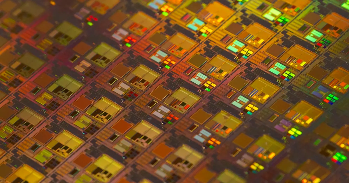
Moore’s Law is the observation, credited to Intel co-founder Gordon Moore, that the number of transistors that can be economically packed onto a chip roughly doubles every couple of years. It isn’t a law of physics — it’s an empirical trend describing how fast manufacturing technology improved, and it held remarkably well for decades, becoming the baseline assumption the entire computing industry planned around.
What doubling transistor count actually bought
More transistors on the same size of chip means each individual transistor is smaller. Smaller transistors switch faster and use less energy per switch, which for a long stretch of computing history translated fairly directly into faster clock speeds and lower power consumption from one generation of chips to the next — largely without engineers having to redesign how a chip worked, just by shrinking the manufacturing process.
That direct relationship between smaller transistors and faster, more efficient chips is sometimes discussed alongside Dennard scaling, a related and now largely broken-down trend that specifically covered power density staying roughly constant as transistors shrank. Dennard scaling’s breakdown in the mid-2000s is a big part of why clock speeds stopped climbing the way they had in prior decades even while transistor counts kept increasing — chipmakers could still pack in more transistors, but not without running into heat and power limits that raw frequency increases used to sidestep. That shift is a large part of why the industry moved toward packing more processing cores onto a chip instead of just pushing a single core faster, and toward specialized silicon like the GPU and the NPU that trade general-purpose flexibility for efficiency on a narrower set of workloads.
Why the trend is slowing
Shrinking transistors indefinitely runs into physical limits, not just economic ones. As transistor features approach the scale of a handful of atoms, effects like quantum tunneling — electrons passing through barriers that should classically block them — make it harder to keep a transistor reliably in an “on” or “off” state. Heat density is also a persistent constraint: packing more switching transistors into the same area generates more heat in the same space, and dissipating that heat becomes progressively harder as the chip’s surface area doesn’t shrink along with the transistors on it.
Manufacturing cost is the other half of the slowdown. Each new generation of smaller transistors requires progressively more advanced and more expensive fabrication equipment and processes. The cost per transistor, which fell steadily for decades, has flattened and in some cases reversed at the most advanced process nodes — a shift that reshapes the economics Moore’s Law originally described, since the “law” was always as much about economical density as raw technical feasibility.
A related idea: Moore’s Law is about density, not just speed
It’s worth separating what Moore’s Law actually predicts from what people often assume it predicts. The original observation is specifically about transistor density — how many transistors fit economically on a chip of a given size — not directly about clock speed, single-threaded performance, or any other downstream metric. For much of computing history those things moved together closely enough that “Moore’s Law” got used loosely as shorthand for “computers keep getting faster,” but the breakdown of Dennard scaling is exactly the point where that loose usage stopped matching reality: transistor density kept increasing for years after clock speed growth had already largely stalled, because the chip designs using those extra transistors shifted toward more cores and more specialized units rather than a single faster core.
How the industry kept gains coming anyway
Even as pure transistor shrinking slowed, several other approaches have kept overall compute capability climbing:
- Specialized silicon. Instead of one general-purpose processor doing everything, workloads increasingly run on chips designed for a narrower task — see the tradeoffs across CPU vs GPU vs TPU for how purpose-built architectures extract more useful work per transistor for specific kinds of computation than a general-purpose design can.
- Chiplets and packaging. Rather than building an ever-larger single piece of silicon, modern chip designs increasingly combine several smaller chiplets in one package, connected by fast on-package interconnects — a way to keep scaling effective compute without needing a single monolithic die to keep shrinking.
- Memory architecture changes. Stacking memory dies vertically and placing them physically closer to compute, as in HBM, reduces the energy and time cost of moving data — increasingly the real bottleneck in many workloads, rather than raw transistor switching speed.
- Open instruction set architectures. Approaches like RISC-V let designers customize an instruction set for a specific workload rather than paying the overhead of a general-purpose architecture, extracting efficiency gains through design rather than through smaller transistors.
Why it still matters as a concept
Moore’s Law is useful less as a precise forecasting tool today and more as a historical reference point for why computing got dramatically cheaper and more capable for so long, and as a lens for understanding the current shift in strategy. When raw transistor scaling was reliable and predictable, it made sense for the industry to compete primarily on process node improvements. As that scaling has slowed, competition has visibly shifted toward architecture, packaging, and workload-specific design — the set of approaches above — because that’s where the efficiency gains are now easier to find.
The takeaway
Moore’s Law described decades of roughly predictable transistor density doubling, which for a long stretch translated directly into faster, cheaper, more efficient chips. Physical limits like quantum tunneling and heat density, combined with rising manufacturing costs at the most advanced process nodes, have slowed that trend considerably. The industry has responded by shifting where efficiency gains come from — specialized silicon, chiplet packaging, smarter memory architecture, and custom instruction sets — rather than relying on transistor shrinking alone to keep compute capability climbing.
Tagged
Keep reading
 Chisato · · 4 min read
 What Is SerDes? Serializer/Deserializer Chips Explained
SerDes converts parallel data to a serial stream for transmission and back, letting chips move data over fewer, faster wires with less overhead.
 Chisato · · 4 min read
 DRAM vs SRAM: How the Two Main Memory Types Differ
DRAM stores each bit as a charge in a capacitor that needs constant refreshing; SRAM stores each bit in a transistor circuit that holds its state.
 Chisato · · 4 min read
 Von Neumann vs Harvard Architecture Explained
Von Neumann shares one memory for code and data; Harvard architecture splits them. How the two computer architectures differ, and where each is used.