How Computer Chips Are Made: Wafer to Package
Chip fabrication turns a silicon wafer into a working processor through photolithography, etching, doping, and packaging — here's the full process.
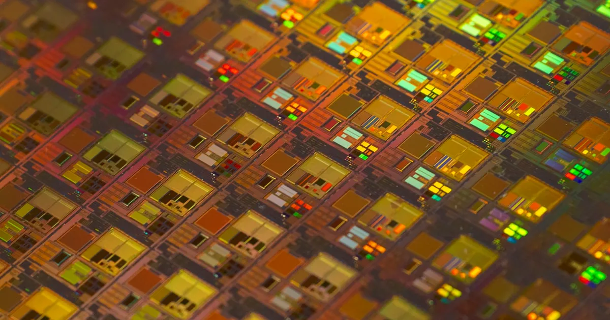
Making a computer chip means building up to dozens of microscopic layers of circuitry on a thin disc of purified silicon, one layer at a time, through a repeating cycle of light exposure, chemical etching, and material deposition — a process that can take weeks from raw wafer to finished chip, even though each individual step happens in seconds.
The chip that ends up in a laptop or a data center server started as sand, and understanding the steps between the two explains why fabs cost tens of billions of dollars and why a process node shrink is such a slow, expensive undertaking.
From sand to wafer
Silicon starts as quartz sand, refined into extremely pure polysilicon — impurity levels are measured in parts per billion, since even trace contamination disrupts a transistor’s electrical behavior. The purified silicon is melted and a single crystal is slowly pulled from the melt (the Czochralski process), producing a cylindrical ingot. That ingot is sliced into thin, mirror-polished discs — wafers — typically 300mm in diameter for modern fabs.
The wafer itself does nothing yet. It’s a blank canvas that the rest of the process builds circuitry onto.
Photolithography: drawing the circuit
Photolithography is the step that actually draws a chip’s circuit pattern onto the wafer, and it’s the step EUV lithography improved on:
- A light-sensitive chemical (photoresist) is coated evenly across the wafer.
- Light — deep ultraviolet or, at the smallest nodes, extreme ultraviolet — is projected through a photomask that encodes one layer of the chip’s circuit design, exposing the photoresist in the pattern of that layer.
- The exposed (or unexposed, depending on resist type) photoresist is chemically developed and washed away, leaving a stencil of hardened resist matching the circuit pattern.
This single step is repeated for every layer of the chip — modern processors can have 15-20+ distinct lithography layers, each aligned to sub-nanometer precision against the layers beneath it.
Etching and doping
With the photoresist stencil in place:
- Etching removes the exposed silicon or deposited material not protected by the resist, using either a chemical bath (wet etching) or a reactive plasma (dry etching, more common at modern nodes for its precision). This carves the actual transistor and interconnect structures into the wafer.
- Doping introduces controlled impurities — typically boron or phosphorus — into precise regions of the silicon to alter its electrical properties, creating the p-type and n-type regions that form a transistor’s junctions. This is usually done by ion implantation, firing ions into the wafer at controlled energy and dose.
- Deposition grows or deposits new material — insulating oxide layers, metal interconnects — on top of the existing structure, building the chip upward layer by layer.
After etching, doping, or deposition, the wafer is usually planarized (chemical-mechanical polishing) to flatten it before the next lithography pass, since even nanometer-scale unevenness would throw off the next layer’s alignment.
Building the interconnects
Transistors alone don’t make a working chip — they need to be wired together, and modern chips have many metal interconnect layers stacked above the transistor layer, connecting billions of transistors into functioning logic. These layers get progressively coarser moving up from the transistor layer (which needs the finest features) to the top layers (which carry power and connect to the package, and can afford to be wider).
This layered interconnect structure is also why die size and yield matter so much economically — one defect anywhere in dozens of aligned layers can render that one die non-functional, which is part of why techniques like chiplets exist: smaller dies have a statistically better chance of coming out defect-free than one enormous monolithic die.
Testing and packaging
Once all layers are complete, the wafer goes through wafer sort — every individual die on the wafer is electrically tested in place, before the wafer is even cut apart. This is also where chip binning starts: dies that meet the highest speed and power specs get sorted into premium bins, while dies with minor defects or lower achievable clock speeds get sorted into lower-tier products, rather than being discarded.
The wafer is then diced into individual dies, and functional dies are packaged — mounted onto a substrate, wired to external pins or contact pads, and sealed, turning a bare silicon die into the chip package that actually plugs into a socket or gets soldered to a board.
Why this all takes so long
A modern chip can require several hundred individual process steps, and many of them — lithography exposure, etching, deposition, testing — must happen in a strictly controlled sequence, with the wafer moved between different specialized machines for each step. Combined with the extreme cleanliness requirements (a modern fab’s cleanroom air is thousands of times cleaner than a hospital operating room, since a single stray particle can ruin a die), the whole cycle from raw wafer to finished, tested chip typically takes several weeks, even though the fab runs continuously, 24 hours a day.
The takeaway
Chip fabrication is a repeating loop — coat with photoresist, expose a pattern with light, etch, dope or deposit material, polish flat, repeat — stacked into dozens of aligned layers on a wafer that started as purified sand. Photolithography draws each layer’s pattern, etching and doping shape the transistors, and interconnect layers wire billions of them together before the wafer is tested, diced, and packaged into the chip that ends up on a board. The sheer number of precisely aligned steps is why fabs are so expensive to build and why advancing to a smaller process node is measured in years, not months.
Tagged
Keep reading
 Chisato · · 4 min read
 Wafer-Scale Integration Explained
Wafer-scale integration builds one giant chip from an entire silicon wafer instead of cutting it into dies. How it works and its tradeoffs.
Chisato · · 4 min read What Is Semiconductor Yield?
Yield is the share of chips on a wafer that work. It's the single biggest driver of chip cost, and why new process nodes start out expensive.
 Chisato · · 5 min read
 2.5D vs 3D Chip Packaging Explained
2.5D packaging places dies side by side on an interposer; 3D packaging stacks dies vertically through silicon vias. How advanced packaging works.