2.5D vs 3D Chip Packaging Explained
2.5D packaging places dies side by side on an interposer; 3D packaging stacks dies vertically through silicon vias. How advanced packaging works.
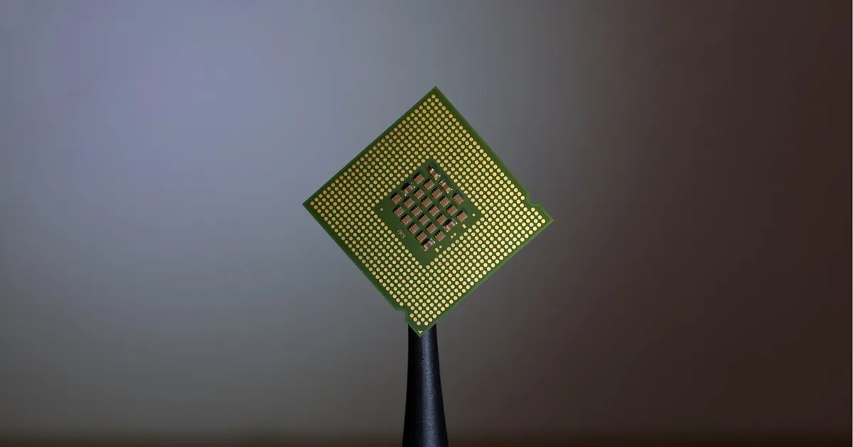
2.5D and 3D packaging are two ways of connecting multiple silicon dies inside a single chip package more tightly than traditional side-by-side packaging allows. 2.5D packaging places separate dies next to each other on a shared interposer, wiring them together through it; 3D packaging stacks dies directly on top of each other, connecting them vertically through the silicon itself. Both are responses to the same pressure: as chiplets replace single monolithic dies, the connections between those chiplets have become as important to performance as anything happening inside them.
Why packaging became a performance bottleneck
For decades, the interesting engineering happened inside the die — smaller transistors, more of them, packed tighter with each new process node. The package around the die was largely a mechanical and electrical afterthought: protect the silicon, route power in, route signals out to the board. As Moore’s law scaling slowed and chipmakers turned to chiplets — smaller dies, each specialized, combined into one package — the connections between those separate dies became a first-class performance concern. A signal traveling between two chiplets across a traditional package substrate is far slower and more power-hungry than one traveling within a single die. Advanced packaging exists to close that gap.
2.5D packaging: side by side on an interposer
In 2.5D packaging, multiple dies sit next to each other on top of a shared piece of silicon — or, less commonly, glass or organic material — called an interposer, rather than being wired directly to the package substrate individually. The interposer carries extremely fine, densely packed wiring, far finer than a standard package substrate can achieve, letting the dies exchange data at much higher bandwidth and lower power than a traditional connection would allow.
This is the packaging style behind most high-end AI accelerators today, which combine a compute die with several stacks of high-bandwidth memory side by side on the same interposer. The “2.5D” name reflects the geometry: the dies themselves are still laid out in a plane, but that plane sits on an intermediate layer that adds a dimension of routing complexity standard packaging wouldn’t otherwise have — not truly stacked in 3D, but not simple flat packaging either.
3D packaging: stacking dies vertically
3D packaging goes further, stacking dies directly on top of one another and connecting them through vertical interconnects that pass straight through the silicon — through-silicon vias, or TSVs — rather than routing signals sideways through an interposer or substrate. This gives the shortest possible electrical path between stacked dies, since the connection is a direct vertical hop instead of a horizontal trip across shared wiring.
High-bandwidth memory is itself a 3D-stacked product internally — multiple DRAM dies stacked and connected with TSVs before that stack is placed, often 2.5D-style, next to a compute die. Some newer designs push 3D stacking further still, placing cache or memory dies directly on top of a compute die’s own active silicon, minimizing the distance between compute and the memory it depends on most.
2.5D vs 3D packaging
| 2.5D packaging | 3D packaging | |
|---|---|---|
| Die arrangement | Side by side, on a shared interposer | Stacked vertically |
| Interconnect path | Through interposer wiring | Through-silicon vias (TSVs) |
| Manufacturing complexity | Lower | Higher |
| Thermal management | Easier — dies share a plane | Harder — heat trapped between stacked layers |
| Bandwidth/latency benefit | Significant over standard packaging | Greatest possible — shortest physical path |
| Common use today | AI accelerators, GPUs with HBM | Memory stacks (HBM itself), cache-on-compute designs |
The tradeoff: bandwidth versus heat
The closer dies sit to each other, the better their electrical connection — and the worse their shared thermal environment gets. A die stacked directly on top of another can’t dissipate heat straight down the way a die sitting flat on a substrate can; heat generated by the bottom die has to pass through, or around, the die stacked above it before a heatsink can remove it. This is the central engineering tension in 3D packaging: it offers the best possible interconnect, but it makes cooling measurably harder, which is part of why 3D stacking has so far been applied more aggressively to lower-power components like memory than to full compute dies running at high clock speeds.
2.5D designs sidestep much of this problem, since side-by-side dies each have their own path to a heatsink, but they pay for it with a longer, less direct interconnect than true 3D stacking offers. Interposer wiring density is also more mature and manufacturable at scale, for now, than dense 3D TSV stacking of large logic dies, which is part of why 2.5D remains the default choice for combining compute and memory dies in today’s highest-volume accelerator designs, while 3D stacking is used more selectively.
Why this matters beyond chip design forums
Advanced packaging decisions show up indirectly in a lot of what determines a chip’s real-world performance: how much memory bandwidth an accelerator can sustain, how much power it burns moving data rather than computing, and how much a manufacturer can charge given how much more complex, and lower-yielding, advanced packaging is compared to traditional packaging. See chip binning for a related concept in how manufacturing imperfections get sorted into different product tiers; advanced packaging adds its own yield challenges on top of whatever the underlying dies already have, since a defect in the interposer or a failed stacking step can ruin an otherwise perfectly good set of dies.
The takeaway
2.5D packaging places multiple dies side by side on a shared interposer, giving them a much faster connection than standard packaging while keeping each die easy to cool; 3D packaging stacks dies directly on top of each other through vertical vias, offering the shortest possible interconnect at the cost of much harder thermal management. Both exist because chiplet-based designs shifted the performance bottleneck from what’s inside a die to how densely and quickly separate dies can talk to each other — and choosing between the two comes down to a tradeoff between interconnect density and how easily the resulting package can shed heat.
Tagged
Keep reading
 Chisato · · 4 min read
 Wafer-Scale Integration Explained
Wafer-scale integration builds one giant chip from an entire silicon wafer instead of cutting it into dies. How it works and its tradeoffs.
Chisato · · 4 min read What Is Semiconductor Yield?
Yield is the share of chips on a wafer that work. It's the single biggest driver of chip cost, and why new process nodes start out expensive.
Chisato · · 4 min read How Computer Chips Are Made: Wafer to Package
Chip fabrication turns a silicon wafer into a working processor through photolithography, etching, doping, and packaging — here's the full process.