Chip Binning Explained: Why One Die Design Sells as Many SKUs
Binning sorts identical die designs by how well each one actually performs after manufacturing, turning natural process variation into a full product lineup.
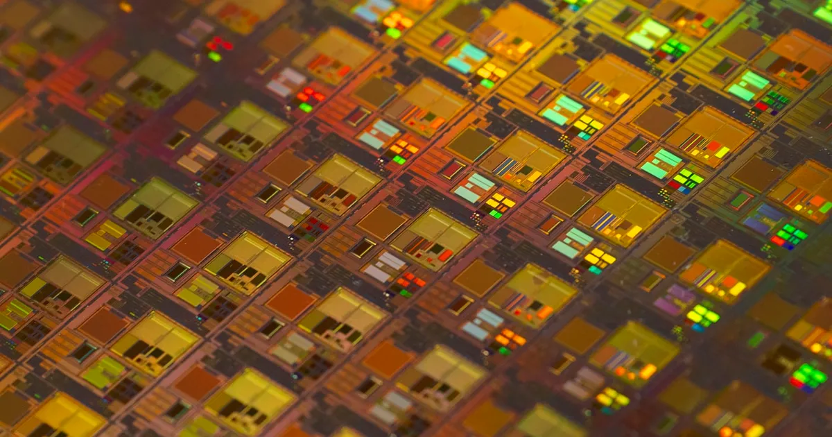
Chip binning is the process of testing every individual die cut from a wafer and sorting (“binning”) it into a product tier based on how it actually performs — its maximum stable clock speed, its power draw, and how many of its cores or functional units work correctly. Chips that started life as the exact same design, built on the exact same process node, routinely end up sold under different model names, at different prices, with different specifications — not because they were designed differently, but because manufacturing variation made them perform differently.
Manufacturing variation is unavoidable
A modern processor die contains billions of transistors, each only a few nanometers across, etched using EUV lithography and dozens of other precision steps. Even with tightly controlled equipment, no two dies come out identical. Minuscule differences in dopant concentration, layer alignment, and etching depth mean that dies from the center of a wafer often perform slightly differently than dies from the edge, and dies from different wafers or production runs vary further still.
The practical effect: some dies can run at a higher clock speed while staying within safe voltage and thermal limits; some run cooler at the same clock speed; some have a defective core or cache segment that fails testing entirely, while the rest of the die works fine. None of this is intentional inconsistency in the design — it’s inherent statistical variation in an enormously precise manufacturing process, and binning is how a manufacturer turns that variation into a coherent product lineup instead of throwing away everything that isn’t perfect.
How the testing process works
After fabrication, every die goes through automated test equipment that pushes it through a battery of checks before it’s packaged and sold:
- Functional testing — does every core, cache bank, and memory controller on the die actually work? A die with one defective core out of eight isn’t necessarily scrapped; it can be sold as a six- or seven-core part with the bad core (and sometimes one working one, for yield-management reasons) permanently disabled.
- Frequency and voltage testing — how high can the die’s clock speed go while remaining stable at a given voltage, and how does that change across a range of operating temperatures? This determines what clock speeds the part can be safely rated for.
- Power testing — how much current does the die draw under load? Some dies leak more current than others due to the same manufacturing variation, which affects both power efficiency and the thermal headroom left for higher clocks.
The results place each die into a “bin” — a category corresponding to a specific SKU with a specific rated clock speed, core count, and power envelope. A die that tests as capable of high clocks with low power draw might become a manufacturer’s flagship part; the same design, with a defective core or middling frequency results, becomes a cheaper, lower-tier SKU instead of scrap.
Why this makes business sense, not just engineering sense
Binning turns a manufacturing reality — not every die is equally capable — into a lineup that serves customers with different budgets and needs, without requiring a separate physical design for each tier. Designing, verifying, and fabricating a distinct die for a budget part and a flagship part would be enormously more expensive than fabricating one design and sorting the output. This is a large part of why a “cut-down” version of a flagship chip (fewer enabled cores, a lower rated clock) so often exists alongside the full part at a lower price — it’s frequently the exact same system-on-chip design, with parts of it disabled because they didn’t meet the flagship bar, not because the budget SKU was engineered separately.
This is also why headroom for overclocking varies so much between individual units of the “same” part — a chip rated for a given clock speed was tested to be reliably stable at that speed with margin to spare, and the amount of margin left over differs from unit to unit purely because of where it came from on the wafer.
Yield and the economics behind it
The percentage of dies from a wafer that pass testing at any usable bin — rather than failing outright — is called yield, and it’s one of the most closely watched numbers in chip manufacturing, because a die that’s fully defective is a total loss of the wafer area and processing cost that went into it. Binning is partly a defect-tolerance strategy: rather than requiring every die to be flawless to be sellable, a manufacturer can recover value from partially defective dies by selling them as lower-tier parts, which materially improves the economics of a process node, especially early in its life when defect rates are typically higher.
This is also why the ratio of high-end to low-end bins shifts as a process matures. Early in a node’s production, imperfections are more common, so a larger share of dies end up in lower bins or fail outright. As the fabrication process is refined over time, yield improves and a larger share of dies qualify for the higher bins — which is one of several reasons flagship-tier parts sometimes become more available, or effective clock speeds creep up, as a given process node matures.
The takeaway
Binning exists because chip manufacturing at nanometer scale can’t produce perfectly identical output from a single design — natural variation in the process means dies test differently for clock speed, power draw, and functional core count even when they came off the same production line. Rather than scrapping every die that isn’t flawless, manufacturers sort tested output into bins that become distinct product SKUs, turning inherent manufacturing variation into a full lineup of pricing and performance tiers built from one underlying design.
Tagged
Keep reading
 Chisato · · 4 min read
 Wafer-Scale Integration Explained
Wafer-scale integration builds one giant chip from an entire silicon wafer instead of cutting it into dies. How it works and its tradeoffs.
Chisato · · 4 min read What Is Semiconductor Yield?
Yield is the share of chips on a wafer that work. It's the single biggest driver of chip cost, and why new process nodes start out expensive.
 Chisato · · 5 min read
 2.5D vs 3D Chip Packaging Explained
2.5D packaging places dies side by side on an interposer; 3D packaging stacks dies vertically through silicon vias. How advanced packaging works.