What Is Semiconductor Yield?
Yield is the share of chips on a wafer that work. It's the single biggest driver of chip cost, and why new process nodes start out expensive.
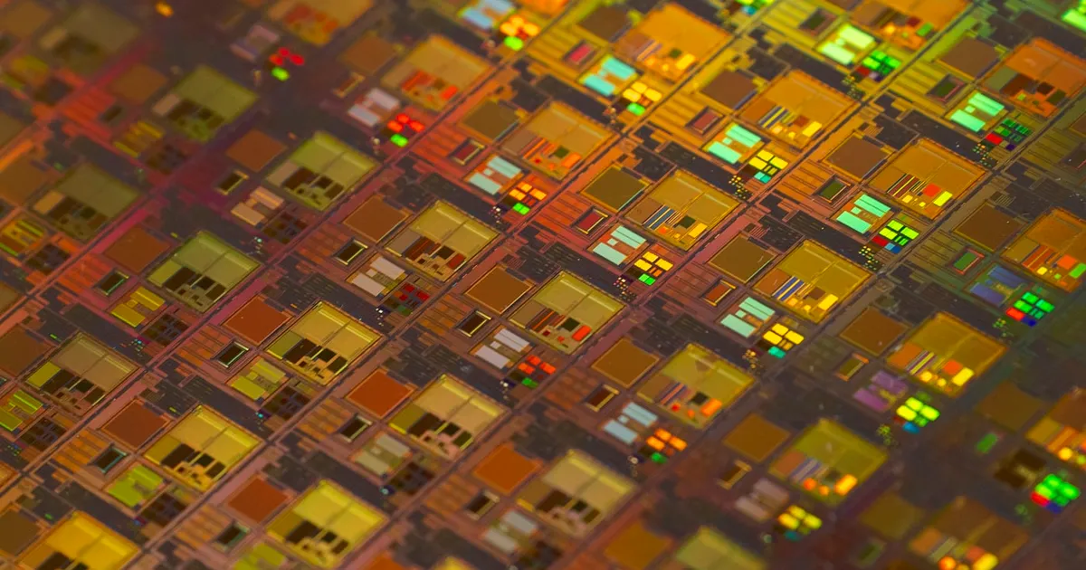
Semiconductor yield is the percentage of chips (dies) cut from a manufactured wafer that actually work correctly, out of the total number of dies the wafer’s size and the chip’s design allow for. A fab running at 90% yield gets nine usable chips for every ten it attempts; one running at 40% yield throws away six out of every ten. Because every wafer costs roughly the same to process regardless of how many good chips come out of it, yield is one of the biggest single drivers of what a chip actually costs to produce — see how computer chips are made for the manufacturing process yield acts on.
Why yield isn’t 100%
Chip manufacturing etches billions of transistors onto a wafer through hundreds of precise steps — photolithography, etching, deposition, doping — at feature sizes measured in nanometers. Even microscopic imperfections matter at that scale: a stray particle of dust, a slight variation in a chemical process step, or a defect in the EUV lithography mask pattern can render a die non-functional. No fab process is perfect, so some fraction of dies on every wafer will always fail.
The key variable is defect density — how many defects occur per unit area of wafer, on average. Yield is a direct function of defect density and die size: more defects per square millimeter, or a larger die that has more area exposed to those defects, both mean more dies affected by at least one flaw.
Why die size matters so much
A defect that lands inside a die typically kills that entire die — a fixed cost regardless of the die’s size. But a larger die covers more wafer area, so it has proportionally more chances of containing at least one defect. This creates a strong incentive to keep die sizes small when a process is still maturing, and it’s a major reason large, complex chips (high-end GPUs, big server processors) tend to have lower yields than small, simple ones manufactured on the same process — there’s simply more silicon area per chip for a defect to land in.
This same math is part of why chipmakers increasingly split large designs into smaller pieces called chiplets connected together rather than manufacturing one giant monolithic die — a chiplet’s smaller area yields better, even though the multi-chip assembly adds its own packaging complexity, discussed in 2.5D vs 3D chip packaging.
The yield curve over a process node’s life
Yield isn’t fixed for a given manufacturing process — it improves over time as a fab tunes and stabilizes the process. A newly introduced process node typically starts with relatively low yield, since the tooling, chemistry, and equipment calibration are all still being refined against real production runs rather than test wafers. As engineers identify and fix the dominant sources of defects, yield climbs — often substantially — over the following months and years, a pattern generally referred to as the yield curve or yield ramp.
This is a major reason new process nodes are expensive when they first launch and why chip designers who want the newest process typically pay a premium: they’re absorbing part of the cost of a process that hasn’t yet reached its mature yield level. It’s also why product lines built on a mature, well-yielding older node can remain cost-competitive for cheaper products long after a newer node exists, even though the newer node offers better performance or density.
Binning: making use of imperfect dies
Not every functional die performs identically — manufacturing variation means some dies run faster, cooler, or with more working cores than others, even from the same wafer and design. Rather than discarding every die that doesn’t meet the top specification, manufacturers sort working dies into different product tiers based on measured performance, a practice called binning. A die with one defective core on an eight-core design, for instance, might be sold as a six-core product with the damaged cores disabled rather than scrapped entirely. See chip binning explained for how this process turns partially-defective silicon into a usable product line instead of pure waste, effectively acting as a yield-recovery mechanism on top of raw pass/fail yield.
Yield’s effect on chip economics
| Factor | Effect on yield | Effect on cost |
|---|---|---|
| Larger die size | Lower — more area exposed to defects | Higher cost per good die |
| Newer, less mature process node | Lower, improving over time | Higher cost early in the node’s life |
| Higher defect density | Lower | Higher cost per good die |
| Redundancy / binning | Recovers otherwise-wasted dies | Lowers effective cost per usable unit |
Because wafer processing cost is largely fixed regardless of outcome, a fab quoting a price per chip is implicitly pricing in its expected yield for that design on that process. This is also why yield figures for cutting-edge nodes are closely guarded — a process node’s actual yield rate is a direct signal of how mature and cost-competitive it is relative to competitors, tied closely to a design’s process node choice.
The takeaway
Semiconductor yield is the fraction of manufactured dies that come out functional, and it’s one of the most consequential numbers in chip economics because wafer processing costs are essentially fixed regardless of how many good chips result. Smaller die sizes yield better because they expose less area to defects, yield improves over a process node’s life as manufacturing matures, and binning recovers value from imperfect-but-functional dies rather than discarding them — all of which is why a brand-new, cutting-edge process is expensive at launch and gets cheaper as the fab dials it in.
Tagged
Keep reading
 Chisato · · 4 min read
 Wafer-Scale Integration Explained
Wafer-scale integration builds one giant chip from an entire silicon wafer instead of cutting it into dies. How it works and its tradeoffs.
 Chisato · · 5 min read
 2.5D vs 3D Chip Packaging Explained
2.5D packaging places dies side by side on an interposer; 3D packaging stacks dies vertically through silicon vias. How advanced packaging works.
Chisato · · 4 min read How Computer Chips Are Made: Wafer to Package
Chip fabrication turns a silicon wafer into a working processor through photolithography, etching, doping, and packaging — here's the full process.