What Is an ASIC? Application-Specific Chips Explained
An ASIC is a chip custom-built for one task, trading flexibility for speed and power efficiency. How ASICs differ from GPUs and FPGAs, and when to use one.
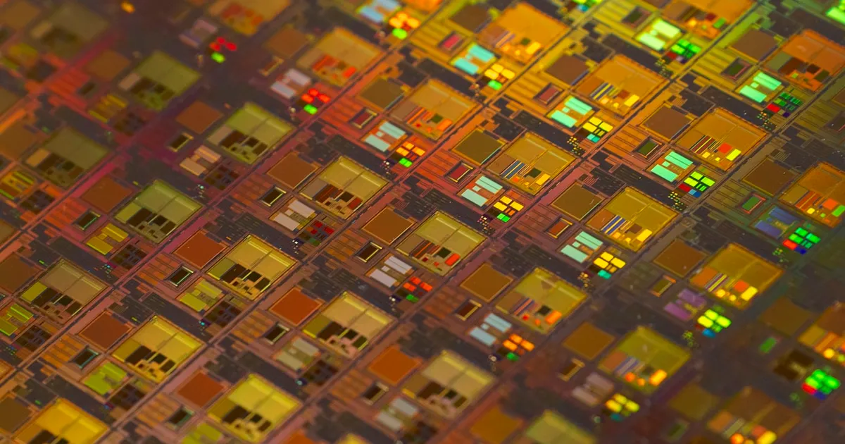
An ASIC (application-specific integrated circuit) is a chip designed and manufactured to do one job, and only that job, rather than being programmed after the fact to run arbitrary code. Where a CPU or GPU is general-purpose silicon that software configures at runtime, an ASIC’s logic is fixed in the layout of its transistors. That specialization is the entire point: give up flexibility and get back speed, power efficiency, and lower per-unit cost at volume.
How an ASIC differs from general-purpose chips
A CPU executes instructions one (or a handful) at a time, decoding each one before acting on it — that decode step is overhead paid on every operation. A GPU is more specialized, built for the specific pattern of thousands of parallel, mostly-identical arithmetic operations, but it’s still a programmable device that runs different GPU kernels depending on the workload.
An ASIC skips programmability entirely. Its circuits implement one algorithm directly in hardware — no instruction fetch, no decode, no general-purpose datapath sized to handle cases it will never encounter. For that one algorithm, an ASIC is dramatically faster and more power-efficient per operation than a CPU or GPU running the same computation in software, because every transistor on the die is doing useful work for that specific task rather than sitting idle for parts of a generic instruction pipeline.
The tradeoff is permanence. Once an ASIC is fabricated, its function cannot change. If the algorithm it implements needs to change — a new hashing function, a new neural network architecture, a new video codec — the chip is obsolete and a new one has to be designed and manufactured from scratch, a process that takes months and a large upfront investment in mask sets and verification.
ASIC vs FPGA vs GPU
This tradeoff sits on a spectrum with two other chip categories, described in more depth in what an FPGA is and CPU vs GPU vs TPU:
| ASIC | FPGA | GPU | |
|---|---|---|---|
| Flexibility | Fixed at fabrication | Reconfigurable after manufacturing | Programmable via software |
| Performance per task | Highest | Lower than ASIC, higher than general CPU | High for parallel workloads |
| Power efficiency | Highest | Moderate | Moderate |
| Upfront cost | Very high (mask sets, verification) | Moderate (off-the-shelf part) | Moderate (off-the-shelf part) |
| Time to market | Months, one-shot | Days to weeks | Immediate (existing hardware) |
| Best for | Fixed, high-volume, stable workloads | Prototyping, low-to-mid volume, evolving workloads | Broad parallel workloads, still-changing algorithms |
An FPGA occupies the middle ground: it’s built from reconfigurable logic blocks that can be rewired after manufacturing to implement almost any circuit, including something close to an ASIC’s design. That reconfigurability costs area and power compared to a true ASIC doing the same job, but it means the same physical chip can be reprogrammed as requirements change — useful when an algorithm is still evolving or volumes don’t justify a custom mask set.
Where ASICs show up
Cryptocurrency mining. Bitcoin mining ASICs implement the SHA-256 hashing loop directly in silicon, achieving orders of magnitude better hashes-per-watt than running the same computation on a CPU or GPU. This is the canonical ASIC use case: one fixed algorithm, run continuously, at massive scale, where power efficiency directly determines profitability.
AI accelerators. Many companies design custom ASICs for running or training neural networks — chips built around the specific matrix-multiply and accumulate operations that dominate deep learning workloads. These sit closer to the ASIC end of the spectrum than a general-purpose GPU, trading some flexibility across different model architectures for better performance-per-watt on the operations that matter most.
Networking equipment. Routers and switches use ASICs to forward packets at line rate — parsing headers and making forwarding decisions in hardware fast enough to keep up with multi-gigabit or terabit link speeds, something a general-purpose CPU handling the same packet rate in software couldn’t sustain.
Consumer electronics. Video codecs, image signal processors in phone cameras, and audio processing in headphones are frequently implemented as small ASIC blocks embedded within a larger system on chip, handling one well-defined, stable task far more efficiently than a general CPU core would.
Why not just use an ASIC for everything
If ASICs are so much faster and more efficient, the obvious question is why CPUs and GPUs exist at all. The answer is that specialization has a cost beyond the chip itself: design time, verification effort, and fabrication expense that only pays off when the algorithm is stable and the production volume is large enough to amortize a multi-million-dollar mask set across millions of units. For workloads that change frequently, or that don’t run at high enough volume to justify a custom design, a general-purpose chip — or an FPGA as a middle ground — remains the more practical choice. This is also why the semiconductor process node used for an ASIC design matters so much: smaller nodes cost more per mask set, so the volume threshold where a custom ASIC beats an off-the-shelf part keeps rising as fabrication gets more advanced.
The takeaway
An ASIC trades programmability for raw efficiency by hard-wiring one algorithm directly into silicon rather than executing it as software on general-purpose logic. That makes it the fastest, most power-efficient option for a fixed, high-volume, stable workload — mining, packet forwarding, a specific neural network operation — but useless the moment the algorithm needs to change. FPGAs offer a reconfigurable middle ground, and GPUs and CPUs stay the right choice whenever the workload is still evolving or doesn’t run at a volume that justifies a custom design.
Tagged
Keep reading
 Chisato · · 4 min read
 Wafer-Scale Integration Explained
Wafer-scale integration builds one giant chip from an entire silicon wafer instead of cutting it into dies. How it works and its tradeoffs.
Chisato · · 4 min read What Is Semiconductor Yield?
Yield is the share of chips on a wafer that work. It's the single biggest driver of chip cost, and why new process nodes start out expensive.
 Chisato · · 5 min read
 2.5D vs 3D Chip Packaging Explained
2.5D packaging places dies side by side on an interposer; 3D packaging stacks dies vertically through silicon vias. How advanced packaging works.