What Is an FPGA? Reconfigurable Chips Explained
An FPGA is a chip whose logic circuits can be reconfigured after manufacturing, sitting between fixed-function ASICs and general-purpose CPUs in flexibility.
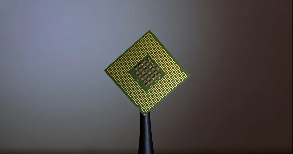
An FPGA, or field-programmable gate array, is a chip whose internal logic circuits can be reconfigured after manufacturing, rather than being fixed at the factory. Where a CPU runs software instructions on fixed hardware, and an ASIC has its logic permanently etched in during fabrication, an FPGA sits in between: you’re programming the hardware itself, and you can reprogram it again later — “in the field,” which is where the name comes from.
How reconfigurable logic works
An FPGA is built from a large array of small, generic building blocks — configurable logic blocks, programmable interconnects, and (on most modern parts) dedicated blocks for memory and arithmetic. None of these blocks does anything useful by default. A configuration file, called a bitstream, tells each logic block what function to perform and tells the interconnect fabric how to wire those blocks together. Load a different bitstream, and the same physical chip becomes a different circuit — a video decoder one day, a network packet filter the next, with no change to the silicon itself.
This is fundamentally different from how a CPU achieves flexibility. A CPU has fixed circuitry and runs varying instructions through it sequentially. An FPGA has varying circuitry itself, and that circuitry can process data in parallel, since a spatial arrangement of logic blocks doesn’t need to take turns the way a CPU’s instruction pipeline does.
FPGA vs CPU vs GPU vs ASIC
Each of these trades flexibility for efficiency differently:
| CPU | GPU | FPGA | ASIC | |
|---|---|---|---|---|
| Flexibility | Highest — runs any software | High — parallel, but SIMD-style | Reconfigurable hardware, not instructions | None — fixed at fabrication |
| Parallelism | Limited (cores) | Massive, thousands of threads | Massive, custom to the design | Massive, custom to the design |
| Power efficiency for a fixed task | Low | Medium | High | Highest |
| Time to deploy a new design | Immediate (just software) | Immediate (just software) | Hours to days (reprogram) | Months (fabrication) |
| Unit cost at scale | Low | Medium | High | Low, once volume is high |
An ASIC, discussed in more depth alongside GPUs and TPUs, is the most efficient option for a task that never changes, because every transistor is dedicated to exactly that task with no configurability overhead. But that efficiency only pays off at high volume, since designing and fabricating an ASIC has substantial upfront cost that has to be amortized over many units. An FPGA gives up some of that raw efficiency in exchange for being reprogrammable, which matters enormously when a design is still evolving, when volumes are too low to justify a custom ASIC, or when the hardware needs to adapt to a changing standard or protocol after deployment.
Common use cases
FPGAs show up wherever custom, parallel hardware logic is valuable but committing to a fixed-function ASIC isn’t:
- Prototyping ASIC designs — before committing to an expensive fabrication run, engineers often validate a circuit design on an FPGA first, since mistakes there just mean reprogramming rather than a costly respin.
- Networking equipment — routers, switches, and network interface cards use FPGAs for packet processing at line rate, where fixed but adaptable logic beats a general-purpose CPU on both latency and power.
- Signal processing — radar, software-defined radio, and other applications that need custom, deterministic, low-latency processing of continuous data streams.
- Financial trading systems — some high-frequency trading firms use FPGAs to shave microseconds off order processing, where the reconfigurability lets them adjust logic as strategies change without the lead time of an ASIC.
- AI inference acceleration — FPGAs can be configured as custom accelerators for specific neural network architectures, particularly useful when a workload’s structure is unusual enough that a general-purpose GPU or fixed NPU design isn’t the best fit.
The tradeoffs, honestly
FPGAs aren’t a free win over the alternatives. Programming one requires a fundamentally different skill set than writing software — hardware description languages like Verilog or VHDL, and a mental model of describing circuits rather than sequential logic. Development cycles are typically slower than software iteration, since even reconfiguring a bitstream involves a compilation and place-and-route process that can take much longer than a software recompile. And per-unit cost is generally higher than an ASIC at scale, since you’re paying for reconfigurability you may only need once, during development.
For most software engineers, FPGAs remain a specialized tool reserved for problems that genuinely need custom, parallel hardware logic with the option to change it later — not a general-purpose alternative to CPUs or GPUs.
The takeaway
An FPGA occupies a specific niche in the hardware flexibility spectrum: more adaptable than an ASIC because its logic can be reconfigured after manufacturing, but more power- and cost-efficient than a general-purpose CPU or GPU for a fixed, specialized task once configured. That combination makes it the right tool for prototyping custom silicon, low-latency signal and packet processing, and any workload where the ability to reprogram hardware after deployment outweighs the efficiency an ASIC would offer at scale.
Tagged
Keep reading
 Chisato · · 5 min read
 What Is a Memory Controller?
A memory controller is the circuit that manages every read and write between the CPU and main memory, setting the ceiling on bandwidth and latency.
 Chisato · · 4 min read
 What Is a DPU (Data Processing Unit)?
A DPU is a specialized chip that offloads networking, storage, and security tasks from the CPU. How data processing units fit alongside CPUs and GPUs.
Chisato · · 4 min read What Is a Semiconductor Process Node?
A process node like '5nm' or '3nm' names a chipmaker's manufacturing generation, not a literal measurement anymore. Here's what the number means.