Intel Ships First High-Volume High-NA EUV Chips
Intel is the first to mass-produce logic chips on ASML's High-NA EUV, dual-qualifying select 18A Panther Lake layers. Here's what shipped and why it matters.

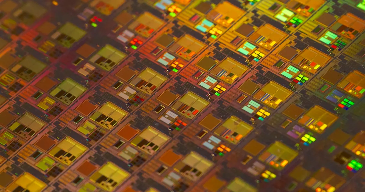
Intel has become the first chipmaker to put the most advanced lithography tool in the industry into real production. On July 15, 2026, ASML confirmed that Intel Foundry is now shipping high-volume logic chips patterned with High-NA EUV — the 0.55 numerical-aperture (NA) successor to standard extreme-ultraviolet lithography — making Intel the first company to move the technology out of the lab and onto commercial silicon. Select layers of Intel’s Panther Lake processors, sold as the Core Ultra Series 3 and built on the Intel 18A node, are now “dual-qualified” to run on both standard 0.33 NA and the new 0.55 NA scanners.
The announcement is narrow in scope but large in symbolism. It is the clearest evidence yet that High-NA EUV — a machine that costs more than its predecessor and had faced open questions about how quickly customers would adopt it — is production-ready, and it hands Intel a concrete claim to process leadership at a moment when the company badly needs one.
What actually shipped
High-NA EUV is not a wholesale replacement for Intel’s existing process. According to ASML and Intel, a subset of Panther Lake layers is being manufactured on High-NA at Intel’s Hillsboro, Oregon site, with the parts shipping to customers at yields matched to the standard NXE platform — the 0.33 NA EUV scanners Intel already runs in volume. The dual-qualification detail matters: it means Intel can build the same design on either tool, giving the foundry flexibility to route wafers to whichever scanner has capacity rather than betting a product line entirely on a single, scarce machine.
The physics behind the upgrade is straightforward. EUV lithography prints circuit patterns using 13.5-nanometer light; the “numerical aperture” describes how tightly the optics can focus that light. Raising NA from 0.33 to 0.55 sharpens resolution enough to print the finest features in a single exposure where the older tools increasingly need multiple patterned passes stitched together. Fewer passes means fewer process steps, fewer chances for defects, and — in principle — faster, cheaper production of the densest layers on a leading-edge chip.
Intel and ASML integrated the industry’s first commercial High-NA system at Hillsboro in 2024, well ahead of rivals, and have spent the intervening period qualifying the tool for manufacturing rather than research. The July milestone marks the transition from that qualification work to shipping product.
Why Intel moved first
Intel’s willingness to be the guinea pig is a deliberate bet. The company has trailed TSMC and Samsung on manufacturing for years, and its turnaround plan hinges on its most advanced nodes — Intel 18A and the roadmap beyond it — regaining a credible technology edge and attracting external foundry customers. Being first on High-NA is the kind of tangible proof point that argument has lacked.
It also aligns with Intel’s broader capacity push. The chipmaker recently committed €5 billion to expand its Leixlip, Ireland campus and has been reshaping its manufacturing footprint around leading-edge demand. Owning the first production High-NA line gives Intel a story to tell prospective foundry clients that neither TSMC nor Samsung can currently match, even if those rivals are expected to bring their own High-NA tools online in the years ahead.
There is a cost side to the ledger. A High-NA scanner carries an even steeper price tag than a standard EUV machine — a reason customers had been cautious about ramping it — and running a subset of layers on the new tool while keeping the rest on 0.33 NA is a measured, risk-managed rollout rather than a full conversion. Intel is proving the tool works at volume without yet committing an entire node to it.
The ASML angle
For ASML, the sole maker of both standard and High-NA EUV systems, Intel’s production ramp is a validation the company has been eager to point to. On its recent Q2 earnings call, ASML leadership cited Intel’s use of High-NA in production as “proof of the maturity of the tool” — a signal to other foundries and memory makers weighing the investment that the technology is ready and that waiting risks ceding a manufacturing edge.
That matters because High-NA is central to ASML’s long-term growth. The company’s most advanced systems command premium prices, and broad adoption across the leading-edge foundries would extend the runway for a business already riding surging demand from the AI chip buildout. Intel going first de-risks the decision for everyone else.
What it means
Intel’s High-NA milestone is a genuine engineering achievement wrapped in a strategic message, and the two should be read together.
Who wins. Intel gets the headline it has wanted for years: a manufacturing first that rivals cannot claim today. For a foundry business trying to convince customers it belongs on the leading edge, “first to ship High-NA logic in volume” is a marketing line backed by real wafers. ASML wins too, gaining the reference customer that turns a high-priced, unproven tool into a validated one — useful leverage as it pitches the same machines to TSMC, Samsung, and the memory makers.
What’s still unproven. The rollout is deliberately partial. Only a subset of Panther Lake layers runs on High-NA, and yields are described as matched to the existing platform rather than better — meaning the immediate benefit is capability and future headroom, not a step-change in cost or performance today. The economic payoff from single-exposure patterning shows up as designs get denser and as Intel widens High-NA use across more layers and future nodes. Until then, this is a foundation, not a finished advantage.
What to watch. Three things. First, whether Intel expands High-NA to more layers and to nodes beyond 18A, which would signal real confidence in the tool’s economics. Second, how quickly TSMC and Samsung respond — their adoption timelines will determine whether Intel’s lead is a durable edge or a brief window. Third, external foundry wins: the ultimate test of Intel’s turnaround is not shipping its own chips on a first-of-its-kind tool, but persuading outside customers to build theirs there too. This milestone gives Intel a stronger pitch. Whether it converts into signed foundry business is the story that actually moves the company.
Tagged
Keep reading
 Chisato · · 4 min read
 Wafer-Scale Integration Explained
Wafer-scale integration builds one giant chip from an entire silicon wafer instead of cutting it into dies. How it works and its tradeoffs.
 Chisato · · 4 min read
 What Is HBM? High Bandwidth Memory Explained
HBM stacks DRAM dies vertically and connects them through a wide interface, trading capacity per chip for far higher bandwidth than standard DRAM.
 Chisato · · 4 min read
 What Is Dennard Scaling? Why Clock Speeds Stopped Climbing
Dennard scaling held that shrinking transistors kept power density constant, letting clock speeds rise for free. Its breakdown reshaped chip design.