What Is Silicon Photonics? Optical Chips Explained
Silicon photonics moves data with light instead of electrical signals on standard chip manufacturing lines. How it works and why AI data centers need it.
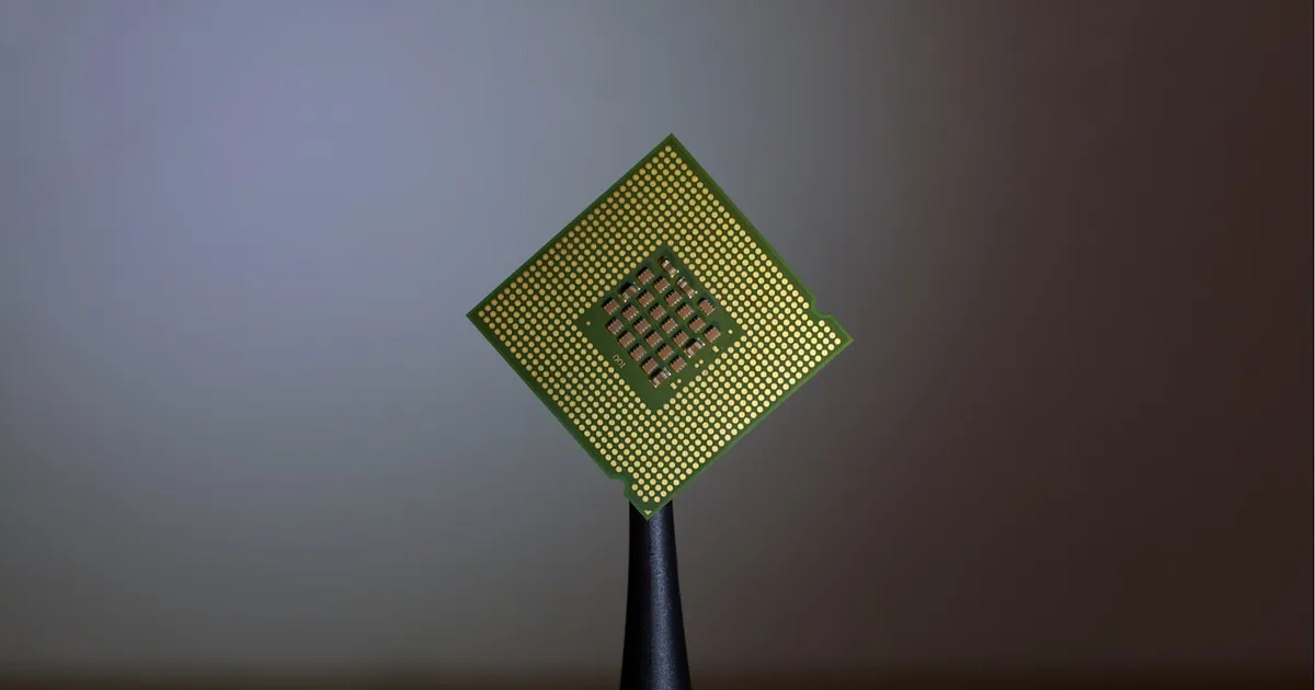
Silicon photonics is a manufacturing approach that builds optical components — waveguides, modulators, and photodetectors that transmit and process data as light rather than electrical current — directly onto silicon chips, using the same lithography processes that produce conventional electronic chips. It’s the technology that lets data centers move enormous amounts of data between chips and racks using light instead of copper, without abandoning the mature, high-volume manufacturing infrastructure the semiconductor industry has spent decades building around silicon.
Why move data with light instead of electricity
Electrical signals moving through copper wires face two compounding problems as data rates climb and distances grow: signal loss (attenuation) increases with distance and frequency, and electrical interconnects consume more power per bit as speeds increase, generating heat that has to be removed. Light traveling through an optical fiber or waveguide doesn’t suffer nearly the same attenuation over distance, and moving a bit optically over a longer link costs meaningfully less energy than pushing the equivalent electrical signal through copper at the same speed.
This tradeoff has been well understood for decades — it’s why long-haul internet backbones have used fiber optics since the 1980s. What’s changed is the distance at which it starts paying off. As chip-to-chip and rack-to-rack bandwidth demands in AI training clusters have grown far past what copper can efficiently carry, the crossover point where optical interconnects beat electrical ones has moved much closer to the chip itself — from the data center’s outer network down toward the rack, and eventually toward the GPU package itself.
Why silicon, specifically
Optical components have existed for a long time, but they were historically built from exotic materials — indium phosphide, lithium niobate — using specialized, low-volume fabrication processes that made them expensive relative to electronics manufactured at silicon’s massive economies of scale. Silicon photonics’ core insight is that silicon is also a decent optical material at the infrared wavelengths used for data communication, and that photonic structures (waveguides that guide light, ring resonators, and modulators that switch light on and off to encode data) can be patterned into silicon using the same CMOS fabrication tools and processes already used to manufacture logic and memory chips.
That compatibility is the whole value proposition: it means optical components can, in principle, ride the same manufacturing cost curve and process maturity that has driven electronics for decades, rather than requiring a parallel, low-volume supply chain. A silicon photonics device typically still needs a laser light source, which silicon is bad at producing directly — so most designs integrate or attach a separate laser (often built from a III-V semiconductor material better suited to light emission) alongside the silicon-based waveguides and modulators.
Where it shows up in practice
The clearest current application is co-packaged optics: placing the optical transceiver components directly next to — or eventually inside — the same package as a switch chip or GPU, rather than as a separate pluggable module connected by a short length of copper. Shortening that electrical link (or eliminating it entirely) is where most of the power savings come from, since it’s the electrical trace from the switch chip to a transceiver at the edge of the board, more than the transceiver itself, that’s been eating into the power and bandwidth budget.
This matters most acutely for the kind of high-bandwidth, tightly-coupled interconnects used in AI training clusters — the same class of problem that motivates interconnect standards like NVLink and memory technologies like HBM, and that CXL addresses for pooled memory across a rack. Silicon photonics targets a related but distinct layer of that stack: not memory bandwidth within a package, but data movement between packages, boards, and racks, at a scale where copper is running out of runway.
Silicon photonics vs traditional optical transceivers
| Traditional pluggable optics | Silicon photonics / co-packaged optics | |
|---|---|---|
| Manufacturing | Specialized, lower-volume optical fabs | Standard CMOS fabrication processes |
| Physical location | Separate module at the edge of a switch or server | Integrated into or adjacent to the chip package |
| Electrical trace length | Longer — module sits away from the die | Shorter — much of the copper path is eliminated |
| Power efficiency | Lower, due to longer electrical runs | Higher, due to shortened electrical path |
| Maturity | Well-established, widely deployed today | Earlier-stage, ramping in high-end deployments |
The engineering tradeoffs
Co-packaging optics with a switch or compute die isn’t a free upgrade. Lasers generate heat and degrade with temperature, which complicates thermal design when they’re placed close to a hot compute die rather than in a separate, more easily cooled module. Repairability also gets harder: a pluggable transceiver can be swapped in seconds if it fails, while an optical engine soldered into a multi-thousand-dollar package failing means a much costlier repair or replacement. These tradeoffs are part of why the technology has rolled out gradually into the highest-bandwidth-per-dollar use cases first — large-scale AI interconnects and top-of-rack switching — rather than displacing conventional pluggable optics everywhere at once.
The takeaway
Silicon photonics brings optical data transmission onto the same manufacturing processes used for conventional silicon chips, making it economically viable to push light-based interconnects much closer to the compute die than fiber optics have traditionally reached. The immediate payoff is lower power consumption and higher bandwidth for the chip-to-chip and rack-to-rack links that AI training clusters depend on, by shortening or eliminating the power-hungry electrical traces that dominate today’s interconnects. It’s an incremental extension of a decades-old idea — light travels more efficiently than electricity over distance — applied at a distance scale that’s only recently become the bottleneck worth solving.
Tagged
Keep reading
 Chisato · · 4 min read
 Wafer-Scale Integration Explained
Wafer-scale integration builds one giant chip from an entire silicon wafer instead of cutting it into dies. How it works and its tradeoffs.
Chisato · · 4 min read What Is Semiconductor Yield?
Yield is the share of chips on a wafer that work. It's the single biggest driver of chip cost, and why new process nodes start out expensive.
 Chisato · · 5 min read
 2.5D vs 3D Chip Packaging Explained
2.5D packaging places dies side by side on an interposer; 3D packaging stacks dies vertically through silicon vias. How advanced packaging works.