NVLink vs PCIe: GPU Interconnects Explained
NVLink and PCIe both move data to and from GPUs, but NVLink trades PCIe's universality for far higher bandwidth between GPUs specifically.
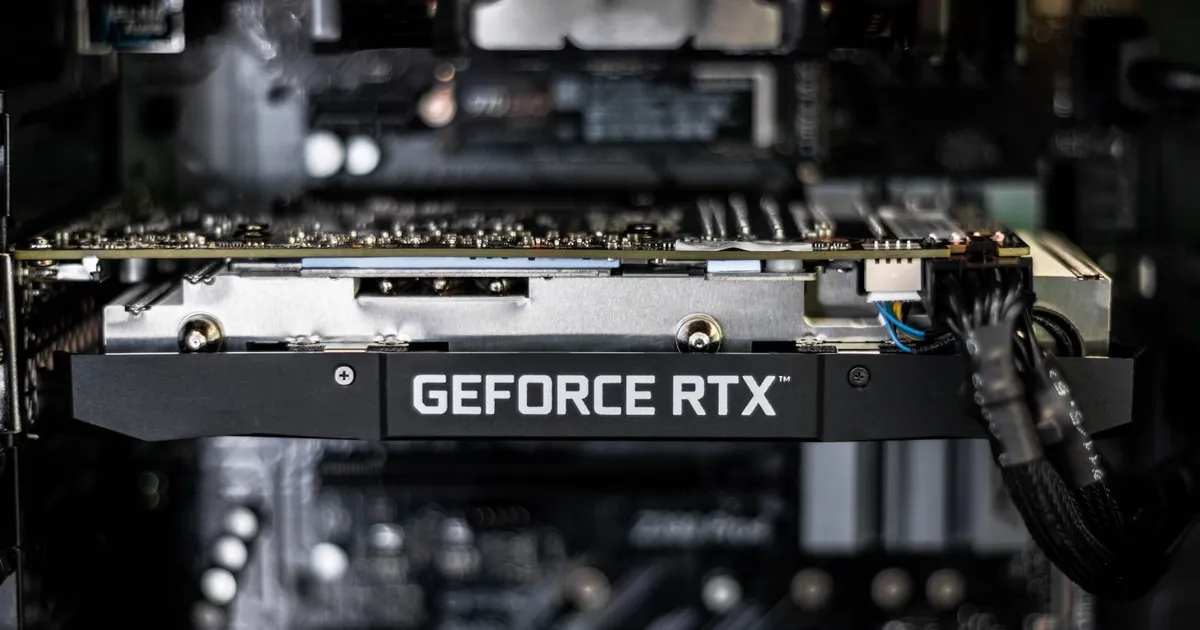
NVLink and PCIe are both interconnects for moving data to, from, and between GPUs, but they solve different problems: PCIe is a general-purpose bus that connects almost any component to a system, while NVLink is a proprietary, higher-bandwidth link built specifically for GPU-to-GPU (and GPU-to-CPU) traffic. A server can — and typically does — use both at once, PCIe for general connectivity and NVLink for the links that matter most for multi-GPU throughput.
What PCIe does
PCIe (Peripheral Component Interconnect Express) is the standard, vendor-neutral bus that connects GPUs, storage, network cards, and other peripherals to a system’s CPU and memory. Every GPU ships with a PCIe interface because it has to interoperate with motherboards, CPUs, and operating systems from any vendor. That universality is PCIe’s strength — and also its ceiling. Bandwidth is shared across whatever’s plugged into the bus, each new generation roughly doubles throughput over the last, and a GPU talking to another GPU over PCIe has to route through the host system’s PCIe topology, often crossing a root complex or switch in the process.
What NVLink does differently
NVLink is a point-to-point interconnect designed to let GPUs talk directly to each other (and, on some platforms, directly to CPUs) at bandwidth well beyond what PCIe offers for the same purpose. Instead of routing GPU-to-GPU traffic through the general-purpose system bus, NVLink provides dedicated high-speed lanes directly between GPU dies, often meshed together with a separate switch chip so that many GPUs can reach each other with consistent, high bandwidth rather than being bottlenecked by whichever GPU happens to sit “between” two others on a shared bus.
The tradeoff is that NVLink is proprietary: it only connects GPUs (and select CPUs) from the same vendor’s ecosystem, and it isn’t a general peripheral bus — you can’t hang a network card or an SSD off an NVLink port. It exists purely to solve the specific, expensive problem of moving enormous amounts of data between GPUs as fast as possible.
Why the distinction matters for AI workloads
Training and running large models increasingly means splitting a single model across multiple GPUs — some layers on one, some on another, or the same layer’s computation split across several. That approach only works well if the GPUs can exchange intermediate results fast enough that communication doesn’t dominate the time spent actually computing. This is the core reason NVLink exists: at PCIe bandwidths, multi-GPU communication becomes the bottleneck long before individual GPU compute does, especially for the all-to-all communication patterns common in distributed training.
A rack of GPUs connected only by PCIe scales poorly past a handful of devices working together closely; the same GPUs connected by a dedicated interconnect and switch fabric scale much further, which is why high-end AI training and inference systems lean so heavily on proprietary GPU interconnects rather than treating PCIe as sufficient.
NVLink vs PCIe at a glance
| PCIe | NVLink | |
|---|---|---|
| Scope | General-purpose peripheral bus | GPU-to-GPU (and select GPU-to-CPU) only |
| Vendor | Open standard, universal | Proprietary |
| Typical use | Connecting GPUs, storage, NICs to a host | High-bandwidth links between GPUs in a node |
| Topology | Shared bus / tree via root complex | Point-to-point mesh, often via a dedicated switch |
| Where it shines | Compatibility across any system | Multi-GPU training and inference at scale |
Where CXL fits alongside them
It’s also worth distinguishing this from CXL, which runs over the same physical PCIe layer but adds cache-coherent memory sharing on top — letting a CPU and an accelerator, or multiple devices, share and coherently access the same memory pool. CXL and NVLink both aim at problems PCIe alone doesn’t solve well, but from different angles: CXL generalizes memory sharing across a coherent domain, while NVLink specializes in raw GPU-to-GPU bandwidth for a specific vendor’s hardware.
Memory bandwidth is a related, separate concern
NVLink bandwidth is easy to conflate with a GPU’s own memory bandwidth — how fast the GPU reads and writes its own attached memory, typically HBM rather than SRAM or conventional DRAM. These are different numbers solving different problems: memory bandwidth governs how fast a single GPU can feed its own compute units, discussed in more depth in memory bandwidth vs. latency, while interconnect bandwidth governs how fast that GPU can exchange data with its neighbors. A model that’s memory-bandwidth-bound on a single GPU won’t be fixed by a faster interconnect, and vice versa — diagnosing which one is the bottleneck matters before investing in either.
Where this is headed
As GPU count per training run keeps climbing, the interconnect between GPUs — not the GPUs themselves — increasingly determines how well a system scales. This is part of why systems built for large-scale AI training bundle many GPUs, a dedicated NVLink-style switch fabric, and high-bandwidth memory together as a package, rather than treating interconnect as an afterthought bolted onto commodity PCIe slots. It also explains why competing accelerator vendors have pursued their own high-bandwidth interconnect standards rather than relying on PCIe alone for multi-chip scaling.
The takeaway
PCIe is the universal bus every GPU speaks to be compatible with the rest of a system; NVLink is a specialized, high-bandwidth link built specifically to move data between GPUs faster than PCIe can. They’re complementary, not competing — real systems use PCIe for general connectivity and NVLink (or an equivalent proprietary fabric) for the GPU-to-GPU links where bandwidth actually determines how well a multi-GPU workload scales.
Tagged
Keep reading
 Chisato · · 4 min read
 Wafer-Scale Integration Explained
Wafer-scale integration builds one giant chip from an entire silicon wafer instead of cutting it into dies. How it works and its tradeoffs.
 Chisato · · 4 min read
 What Is HBM? High Bandwidth Memory Explained
HBM stacks DRAM dies vertically and connects them through a wide interface, trading capacity per chip for far higher bandwidth than standard DRAM.
 Chisato · · 4 min read
 Thermal Interface Materials Explained
Thermal interface material fills microscopic gaps between a chip and its heatsink so heat can actually transfer to the cooler.