What Is a Northbridge and Southbridge? The Chipset
The northbridge and southbridge were the two chips that routed data between a CPU, memory, and peripherals before modern SoCs absorbed their jobs.
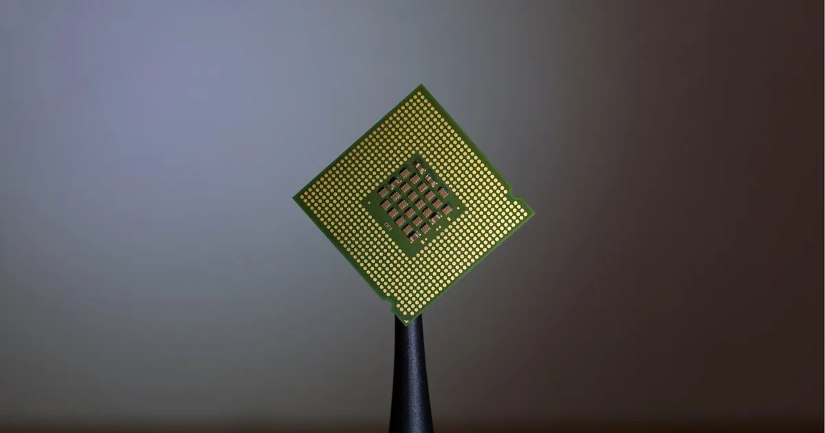
The northbridge and southbridge were the two chips that, together, formed a PC motherboard’s chipset — the circuitry responsible for routing data between the CPU, memory, and every peripheral device. The split organized the motherboard’s traffic by how fast and how latency-sensitive each connection needed to be, with the northbridge handling the fast stuff close to the CPU and the southbridge handling everything else. Most of what they did has since been absorbed into the CPU package itself, but the split is still the clearest way to understand how a computer’s internal traffic is organized.
The northbridge: the fast lane
The northbridge sat physically closest to the CPU on the motherboard and handled the connections that needed the most bandwidth and the lowest latency:
- Memory controller — the link between the CPU and system RAM, translating memory requests into the timing and signaling a DRAM module needs.
- Graphics interface — historically AGP, later PCIe, connecting to the graphics card.
- CPU-to-chipset link — the front-side bus or equivalent, carrying everything that wasn’t handled directly by the CPU itself.
These connections shared one property: they were all latency-sensitive enough that routing them through a second hop would have hurt performance noticeably. Keeping the northbridge physically close to the CPU minimized the trace length — and therefore the signal delay — on these high-speed links.
The southbridge: everything else
The southbridge handled the slower, less latency-critical peripherals — the input/output side of the system:
- USB controllers
- SATA/storage controllers
- Audio codecs
- Legacy interfaces like the old PCI bus, serial and parallel ports
- The BIOS/firmware interface
None of these needed the northbridge’s tight latency budget, so they were grouped onto a separate chip connected to the northbridge by a slower internal link (commonly called DMI or a similar interconnect, depending on the platform), rather than competing for bandwidth on the CPU’s direct path.
Why the split existed
The two-chip design was a pragmatic response to how fast different parts of a system needed to move data, at a time when integrating everything onto the CPU die wasn’t practical. Splitting the chipset let motherboard vendors mix and match — pairing a given CPU generation with different southbridges to offer different peripheral feature sets, without needing to redesign the performance-critical northbridge. It also kept the highest-speed signals confined to the shortest possible physical traces, which mattered more as clock speeds climbed and signal integrity became harder to guarantee over longer runs of motherboard trace.
Where the northbridge went
Starting in the mid-to-late 2000s, CPU manufacturers began integrating the memory controller directly into the CPU package — eliminating the northbridge’s main job by moving it onto the same silicon as the processor core. PCIe lanes for graphics followed the same path. This wasn’t a naming change; it reflected a real architectural shift: with the memory controller on-die, the CPU talks to RAM directly instead of routing every memory access through a separate chip, cutting a hop out of the most latency-sensitive path in the entire system.
Where the southbridge went
The southbridge’s functions persisted longer as a physically separate chip — now usually called a platform controller hub (PCH) or similar, depending on the vendor — because peripheral I/O is less latency-sensitive and benefits less from being pulled onto the CPU die. But the trend has continued in the same direction: modern systems-on-chip, especially in laptops and mobile devices, integrate storage, USB, and even some peripheral controllers directly into a single package alongside the CPU and GPU, leaving a discrete southbridge-equivalent chip mostly in desktop and workstation designs that still value modularity over integration.
Why the concept still matters
Even where the physical two-chip split no longer exists, the underlying idea — separating a system’s fast, latency-critical data paths from its slower, more flexible peripheral paths — persists inside modern SoC designs, just implemented as separate blocks and interconnects on a single die rather than separate chips on a board. Understanding the northbridge/southbridge split is a useful mental model for reading any modern chip diagram: some paths are optimized for raw speed to memory and the GPU, and others are optimized for flexibility and device count, and that distinction hasn’t gone away even as the physical chips have merged.
The takeaway
The northbridge handled the CPU’s fastest, most latency-sensitive connections — memory and graphics — while the southbridge handled slower peripheral I/O. Rising clock speeds and the practical benefits of shorter signal paths eventually pushed the northbridge’s job onto the CPU die itself, and the southbridge’s functions have followed the same trajectory into modern platform controller hubs and SoCs. The two-chip chipset is largely a historical artifact now, but the traffic-shaping logic behind it — separate fast and slow paths — is still how chip architects think about routing data today.
Tagged
Keep reading
 Chisato · · 4 min read
 What Is HBM? High Bandwidth Memory Explained
HBM stacks DRAM dies vertically and connects them through a wide interface, trading capacity per chip for far higher bandwidth than standard DRAM.
 Chisato · · 4 min read
 Thermal Interface Materials Explained
Thermal interface material fills microscopic gaps between a chip and its heatsink so heat can actually transfer to the cooler.
Chisato · · 4 min read What Is Dennard Scaling? Why Clock Speeds Stopped Climbing
Dennard scaling held that shrinking transistors kept power density constant, letting clock speeds rise for free. Its breakdown reshaped chip design.