High Bandwidth Flash: First HBF Standard Released
Sandisk and SK hynix published the first OCP technical spec for High Bandwidth Flash, a stacked-NAND memory aimed at the AI inference capacity wall.
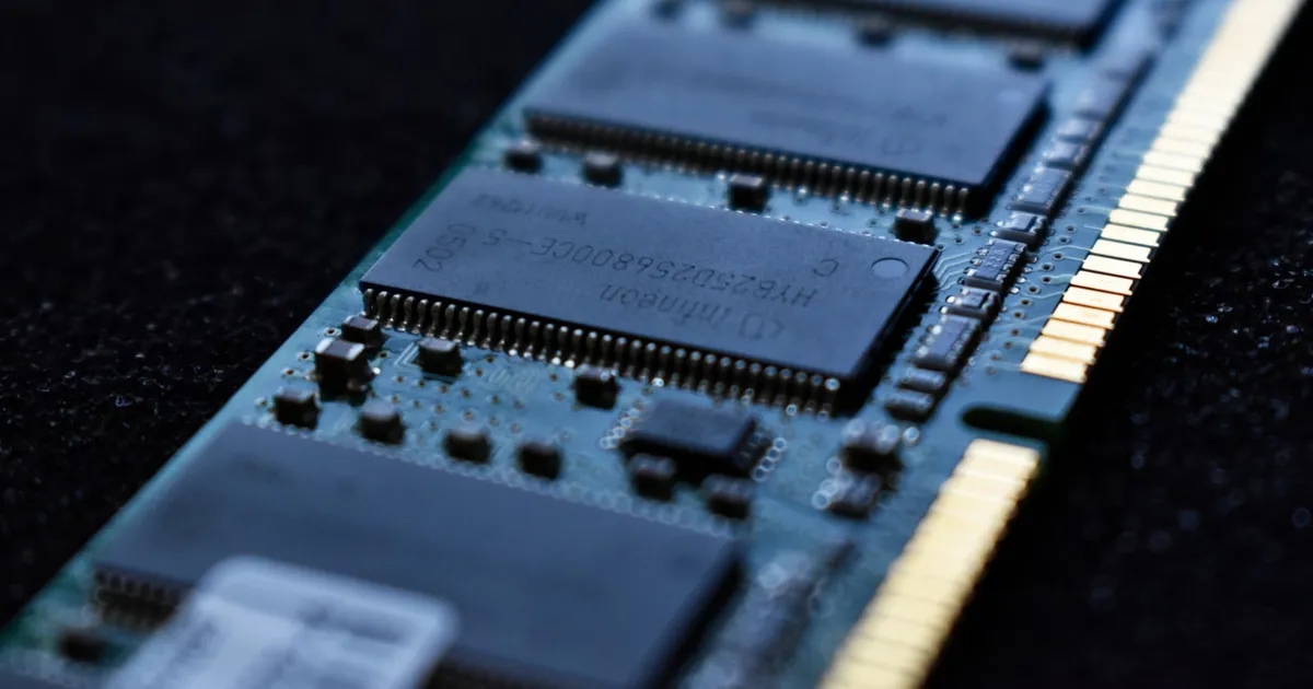
The memory industry took its first formal step toward a new class of AI chip on Monday. On August 3, 2026, Sandisk and SK hynix said they had published the inaugural technical specification for High Bandwidth Flash (HBF) through the Open Compute Project (OCP), the vendor-neutral consortium that standardizes data-center hardware. The document turns what had been a two-company research effort into an open blueprint that any accelerator designer can build against — and it arrives just six months after the OCP workstream began in February.
HBF is a bid to solve one of the most stubborn constraints in modern AI: not how fast a chip can compute, but how much data it can hold close enough to feed those computations. The two memory makers unveiled the specification at the Future of Memory and Storage (FMS) 2026 conference, and disclosed that Google and Tenstorrent had joined the effort as contributors during standardization.
What HBF actually is
HBF borrows the physical playbook of High Bandwidth Memory (HBM) — the stacked DRAM that sits beside GPUs and feeds them data — and applies it to NAND flash, the non-volatile storage found in SSDs. Where HBM stacks DRAM dies to deliver enormous bandwidth over a short, wide interface, HBF stacks NAND dies to deliver far more capacity at bandwidth close to HBM’s, trading a measure of speed and write endurance for a large multiple of storage per package. For the mechanics of why stacked memory commands its premium, our explainer on what HBM is covers the fundamentals HBF inherits.
According to the specification, the first release supports capacities of up to 512GB per stack using 8-high and 16-high NAND configurations. It defines three bandwidth tiers, labeled Grade 1 through Grade 3, spanning roughly 0.4TB/s to 3.0TB/s. Reporting on the spec noted that the design leans on the UCIe die-to-die interconnect and an xPU-HBF host interface — deliberately generic language, since “xPU” is meant to cover GPUs, custom accelerators, and other AI silicon rather than any single vendor’s part.
The document itself is not a product. It defines the system interface, electrical guidelines, reliability and packaging guidance for an HBF die stack, basic performance expectations, and a software user guide for read and write operations. In other words, it is the contract that lets a chip designer, a memory supplier, and a packaging house all build to the same target without bilateral negotiation — the same role JEDEC and OCP specifications have played for DRAM and HBM.
The problem it targets
The pitch for HBF is aimed squarely at AI inference, the phase where a trained model answers queries rather than learns. Inference is increasingly bounded by memory capacity: today’s largest models, long context windows, and key-value caches all need to keep enormous amounts of data resident and reachable at high speed. HBM delivers the bandwidth, but it is expensive and capacity-limited; standard SSD storage offers capacity but sits too far from the processor to feed it at the rates inference demands.
HBF is positioned in the gap between them — a tier that offers HBM-class bandwidth at multiples of HBM’s capacity, letting a single accelerator hold far larger models or longer contexts on-package. Tom’s Hardware framed the approach as a way to give GPUs “terabytes of extra memory” without the die-area and cost penalties of an all-HBM design. The distinction between latency-sensitive and throughput-oriented workloads is the same one we covered in batch vs. real-time inference: HBF is a better fit for capacity-hungry, throughput-oriented serving than for the tightest low-latency paths.
That framing also explains the participant list. Google, which designs its own TPU accelerators, and Tenstorrent, a startup building AI processors, are exactly the kind of customers who would benefit from a memory tier they can design into custom silicon. Their involvement during standardization — rather than after — signals that HBF is being shaped around real accelerator roadmaps, not proposed in a vacuum.
Why standardize first
The most notable thing about Monday’s announcement is the sequence: a published open standard before a shipping product. That is a deliberate move. HBM’s history shows that a fragmented, proprietary memory interface slows adoption; a common specification lets multiple suppliers, packaging partners, and accelerator vendors invest with confidence that their parts will interoperate.
By routing HBF through OCP under a permissive, open process, Sandisk and SK hynix are trying to avoid a single-vendor lock-in narrative and instead recruit the broader ecosystem early. It is also a competitive signal in a market where HBM supply is the choke point for AI hardware. As the memory cycle has repeatedly shown — from the HBM4 supply race to SK hynix’s own HBM4 ramp decisions — whoever defines the next memory tier shapes where the profits and the bottlenecks land next.
The caveats
HBF is not a drop-in HBM replacement, and the companies are not claiming it is. NAND flash has higher latency and finite write endurance compared with DRAM, which is why the specification frames HBF as a capacity tier for read-heavy inference rather than a substitute for the fast working memory HBM provides. Real systems are likely to pair the two: HBM for the hottest, most latency-sensitive data, HBF for the large, relatively static footprint a model needs resident.
There is also a long road from specification to silicon. A published OCP spec is a necessary condition for a broad ecosystem, but it does not by itself deliver validated parts, packaging capacity, accelerators with matching interfaces, or the software stack to manage a new memory tier. The February-to-August timeline is fast for a standards effort; the timeline to volume production and design wins is a separate, longer clock.
What it means
HBF is the memory industry’s answer to a specific 2026 reality: the constraint on serving frontier AI has shifted from raw compute toward how much model you can keep close to the processor, and how cheaply. By publishing an open standard first, Sandisk and SK hynix are trying to make HBF an ecosystem rather than a product — and the early presence of Google and Tenstorrent suggests accelerator designers are taking the capacity wall seriously enough to help define the fix.
The winners, if HBF takes hold, are the NAND makers, who gain a high-value, AI-driven use for flash at a moment when commodity storage economics are unglamorous, and accelerator designers who can offer far larger on-package capacity without paying all-HBM prices. The pressure lands on pure-play HBM as the sole premium AI memory: a viable capacity tier alongside it reshapes the data-center economics that have made high-bandwidth memory the industry’s most prized — and most supply-constrained — component.
What to watch next is concrete: which accelerators announce HBF support, whether Micron and Samsung engage with the OCP effort or counter with their own approach, and how quickly the first Grade-3, 3.0TB/s parts move from specification to samples. A standard is the starting line, not the finish — but for a technology that went from workstream to published spec in six months, the pace itself is the story.
Tagged
Keep reading
 Chisato · · 5 min read
 Samsung LPDDR5X-PIM: In-Memory Compute for AI
Samsung detailed LPDDR5X-PIM at Hot Chips 2026 — a drop-in DRAM that runs AI math inside memory, claiming roughly 3x token throughput and 8x PIM bandwidth.
 Kurumi · · 6 min read
 Korea Chip Exports Hit Record in August, Up 209%
South Korea's chip exports jumped 209% in August 2026 to a record $46.65B — nearly half of all exports — as hyperscaler AI spending drove demand.
 Chisato · · 6 min read
 US Moves to Block China's Remote AI Chip Access
The Commerce Department is drafting a rule to stop Chinese firms from renting banned Nvidia AI compute through data centers in third countries.